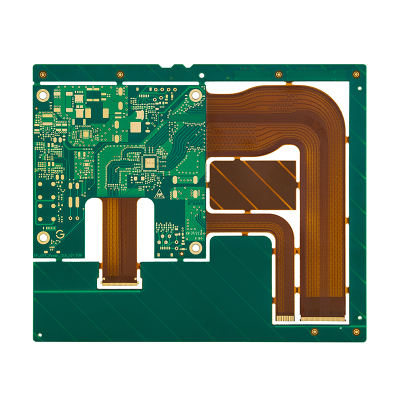
Advanced IC substrates have facilitated a paradigm shift in packaging technology.
“When will glass replace copper clad laminate on advanced IC substrates?” PCB Suppliers

That’s a question many on the heterogeneous integration (HI) side of the semiconductor industry are asking. Unfortunately, the answer is not straightforward.
But before we get to answering that, let’s take an advanced IC substrate (AICS) refresher. In other words, how did we get to the point where glass substrates have become a topic of discussion?
AICS provides a means to connect chiplets and passives with extremely high I/O count to the printed circuit board (PCB). In the process, AICS has facilitated a paradigm shift in packaging technology with the introduction of HI. This revolutionary approach to packaging provides a significantly cheaper alternative to silicon interposer technology, which is limited in the package sizes it can support.
The AICS is built around a fiberglass resin core with copper on both sides. This is known as copper clad laminate (CCL). The CCL facilitates the creation of redistribution layers (RDL) that connect through the substrate core with plated through holes (PTH). The RDLs are separated by organic dielectric layers known as build-up films.
To be even more direct: the AICS is essentially the evolution of the PCB. In fact, many of the patterning techniques and materials are very similar but have been extended or replaced with more capable tooling. For instance, laser drilling replaces mechanical drilling to shrink via holes, and lithography steppers replace laser direct imaging (LDI) systems to reduce RDL dimensions and increase productivity.
Currently, the roadmap requirements for AICS have driven the CCL processing far beyond the capabilities of the PCB world. Today, new materials and processes are required to support the next generation of packages, where package sizes exceed 120mm x 120mm and interconnects (RDL) shrink below 5µm line/space (l/s).
As substrate manufacturers continue to push processing technology to match their customers’ advanced packaging roadmaps, they face several technical challenges. The dilemma: how to lower manufacturing costs, while at the same time, not fall behind on next-generation product development.
This is where glass substrates enter the discussion.
Previously, it was thought the glass substrate transition would be when RDL shrinks below 5µm l/s. However, both equipment and processing solutions are readily available that can extend the life of CCL beyond 5µm line/space to potentially 2µm l/s. For instance, new substrate lithography steppers, with higher resolution lenses and advanced alignment algorithms, which can mitigate substrate distortion effects, enable overlay performance hitherto unknown. In addition, next-generation substrate inspection equipment that can detect RDL defects, currently limiting the yield of smaller RDL features, will soon become available.
Fig. 1: Cross section of CCL substrate.
To realize 2µm l/s with CCL, the process flow will need to be modified to support higher resolution RDL features and micro-via patterning (figure 1). Currently, the CCL via layer is defined by laser drilling through an organic dielectric build-up film. This process is limited to supporting vias >30µm l/s. To reach 2µm l/s roadmap requirements, vias will need to shrink to below 10µm; which will require lithographic patterning. The via lithography process will use either liquid or dry film photo imageable dielectric (PID). So, if CCL processing can reach the 2µm l/s node with good yield, then the glass core process will be pushed out to the next node, or overlap with it, depending on the final package requirements (figure 2).
Fig. 2: Cross section of glass core substrate.
The glass core process has a number of advantages over CCL, but chief among them is the stability of glass to provide a flat and distortion-free surface on which to build the RDL and micro vias, enabling even smaller features to be defined.
Of course, glass comes with its own set of challenges; it’s fragile, especially at the large panel sizes being employed today (510mm x 515mm and 600mm x 600mm). The glass substrate is also very thin, <100µm in some cases, which requires sophisticated handling equipment to process the substrate through the various steps without the risk of breakage.
One compromise of interest is a hybrid solution where the large RDL structures are built using the basic CCL process and the fine-line RDL is patterned on a glass substrate, which is affixed to the CCL through copper microbumps (figure 3).
Fig. 3: Cross section of hybrid build substrate.
This hybrid approach combines the best of both CCL and glass approaches. That being said, there is always a compromise. In this case, the extra layers of microbumps create additional process steps along with the inevitable higher cost.
The insatiable demand for increased RDL density and larger packages is going to continue for the foreseeable future. It is only a question of time before substrate manufacturers reach the 2µm l/s technology node. The only question that remains is will CCL or glass get there first and prevail?
Of course, CCL will eventually reach its physical limits. But as with most successful technologies, the process infrastructure inertia, coupled with next generation AICS equipment and software, will not be halted if there is a cost-effective solution that enables the technology roadmap to be achieved sooner, rather than later. If CCL substrates prove to be capable at the 2µm l/s technology node, they will inevitably overlap with glass substrates since the material properties of both lend themselves to different applications, enabling the two processes to coexist.
Name* (Note: This name will be displayed publicly)

Pcb Process Email* (This will not be displayed publicly)